Rigid Flex PCB Process
PCBs are the heart of any electronic product. They are complex structures that must be manufactured to the highest quality standards to ensure that they are able to perform properly and reliably in a wide range of applications. Even a small design flaw or manufacturing error can drastically impact the functionality, performance, and durability of a final product.
One of the best ways to avoid such errors is to work with a reliable and experienced rigid flex pcb manufacturer. An experienced PCB manufacturer will have a thorough understanding of all rigid flex pcb fabrication processes, and they will be able to help you with any challenges that you might face during the development process.
The first step in the rigid flex pcb process is the design and layout stage. This is where the designer will create the schematic diagram, lay out components, and check for any design errors. It is also at this stage that the designer will determine the stack-up for the rigid and flexible sections. The design phase is typically done using high-end CAD software. The result of this phase is a set of gerber files that will provide the roadmap for the fabrication of the rigid flex circuit board.
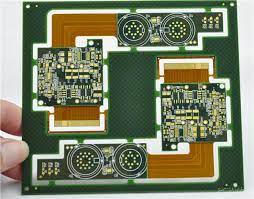
The Rigid Flex PCB Process
Next, the layers of the flex and rigid PCB are laminated together. The flex layer is then imaged and chemically etched, creating the desired circuit patterns. The rigid section is then drilled with the same precision drilling systems and techniques as used in the conventional PCB fabrication process. The copper layer of the flex circuit is then deposited and chemically etched, connecting the rigid and flexible sections of the board. A coverlay is then applied over the etching process, providing an electrical seal for the flexible circuit.
If required, stiffeners are then added to the flex and rigid sections of the board to help prevent damage from flexing or folding. These stiffeners are often made of a polyimide film with adhesive, and they can be patterned using the same screen printing process as rigid board component locations. The coverlay is then laminated to the flex and rigid layers, and the finished rigid flex circuit boards are cut to size.
Depending on your design requirements, you may need to use through-hole components on your rigid flex circuit board. This is where you will need to add holes to the rigid flex board that connect directly to the components on the assembly side. For through-hole components, it is common practice to use a button plating process on the flex ribbon. This allows the through-hole components to be mounted on the flex and then inserted into the hole in the rigid PCB.
The finished rigid flex PCBs are then cut to size, and they are ready for assembly. Before the rigid flex pcb is assembled, it must undergo a thorough inspection to ensure that it meets all of the IPC-610 and IPC-ET-652 requirements for isolation, continuity, reliability, quality, and performance. A rigid flex circuit board that is not compliant with these requirements will not be acceptable for production.